Alena Klindziuk - NanoJapan 2015
Bryn Mawr College
Major: Physics
Class Standing: Sophomore
Anticipated Graduation: May 2018
NanoJapan Research Lab: Prof. Shigehiko Sasa, Department of Electrical and Electronic Systems Engineering, Osaka Institute of Technology
NanoJapan Research Project: ![]()
Why NanoJapan?
What makes NanoJapan special is that it not only gives students an opportunity to conduct exciting nanotechnology research, but also facilitates cross-cultural understanding between scientists. For me, it is a unique chance to not only gain research skills and make a meaningful contribution to the field of THz dynamics, but also learn how to communicate and connect with people of different background and culture. Participating in NanoJapan holds a promise of both academic progress and incredible personal growth.
I am really excited to be given an opportunity to learn about THz dynamics of nanostructures, while being immersed in a professional working environment abroad. I am looking forward to meeting new people, creating friendships and establishing professional connections. Last but not least, I am eager to immerse myself in Japanese culture and learn as much as possible about local traditions, food, history, folklore, industry, art, technology, philosophy, everything! The possibilities are infinite.
My goals for this summer are to:
The first impression I got after arriving in Tokyo was that Japan is very, very clean. The cars, the windows, and even the busses are all specless, while the streets (at least in the Azabu-‐juban area) are completely rid of trash. I have heard that Japan is very clean; however, actually seeing how well-‐maintained the streets are was still very surprising, especially since trash cans are nowhere to be found.
Within the first week, I realized that life in Tokyo has a lot of unexpected perks that I will miss after I return to the US. For example, since everything in Tokyo is so close together, I could find most of my living necessites and much more within a five minutes walk of Sanuki club. Everything from laundry to book shops is within ridiculously close walking distance. Another aspect of Japan that I knew about, but was nevertheless impressed with, is the presence vending machines everywhere. The variety of drinks they provide is amazing -‐ I do not think I can try all of them by August. The beverages they have are cheap and tasty.
Before coming to Tokyo, I thought that living in such a densely populated area might feel claustrophobic. However, after coming here I was pleasantly surprised to find that I did not feel oppressed by the high population density. In fact, precisely because everything is so close together, Tokyo is a very interesting place to live in. Just taking a walk around the block revealed a shrine, an Australian embassy, a cemetery, a small park, a dozen different apartment complexes, and numerous shops of all kinds.
Also, for such a large and dense city, Tokyo has unexpectedly good air quality. I like to keep my window open. It also much greener than I thought it would be. It is clear that the citizens of Tokyo make every effort to grow something green everywhere possible, which I am very grateful for. Walking down the street, one can definitely see that a lot of effort is put into making the capital of Japan the beautiful place it is.
Japanese Classes
Language classes are challenging in that there is much to learn and not much time to study. Another difficulty is in that it is much easier to recall the Japanese vocabulary and sentence structures in class, then when I am out and about. I think that this is due to the lack of practice. Therefore, I make an effort to speak Japanese as much as possible everywhere I go. The hardest part about it, is understanding what the Japanese are saying -‐ they usually speak very fast. My main goal is to improve my Japanese enough to be able to have conversations by the time I have to leave for my lab.
Something Puzzling
As I have already mentioned, the streets of Tokyo are very clean -‐ there is absolutely no trash lying around anywhere. At the same time, trash cans and garbage collection bins can seldom be found. While I can usually stumble upon a bin that collects cans and bottles from the vending machine, I always have to carry other types of trash back to the hotel where I can throw it away. Even walking around the neighborhood, I could not find any garbage disposal bins analogous to those that one sees in the United States. So, I am wondering how does waste disposal work in Japan.
NanoJapan Tip: Here is a good blog post on garbage disposal in Japan but also keep in mind this a security precaution. Public trash bins were removed from Tokyo, especially in subway stations, following a 1995 sarin gas attack by a religious cult. Also, see pg. 42 of the NanoJapan Schedule/Guidebook.
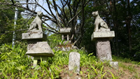
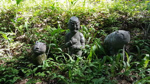
Stone Statues of a Shinto Shrine near Aokimura Farmers carved these stone statues as offerings to gods to pray for prosperity of their village.
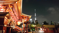
View of Senso‐ji Temple: Sensō‐ji is an ancient Buddhist temple located in Asakusa, Tokyo. It is Tokyo's oldest temple. Tokyo Skytree is clearly visible from its grounds.
Introduction to Nanoscience Seminar
The Intro to Nanoscience Seminars were helpful in providing background information of the science that we are going to need for our projects. The lectures had some material I know and some that was new to me. They were helpful in suggesting what I need to learn more about and read up on. I really enjoyed Dr. Ishioka’s lecture about the ultrafast spectroscopy and her experience of being a woman researcher in Japan. I also found Professor Stanton’s lecture on quantum mechanics very helpful -‐ now I know that I need to review quantum mechanics. Also, I found Professor Kono’s lecture on the Terahertz of Carbon Materials very interesting -‐ it provided a clear background information of THz dynamics.
Intial Research Project Overview
From the articles I received from Sasa-sensei, I learned that I will be working with ZnO-‐based and/or ZnMgO transparent field effect transistors. Basically, my project will involve studying the electrical and opGcal properGes of semiconductor materials present in these transistors. It has been found that the electronic high-‐speed performance of such devices can be improved by opGmizing their structure. Furthermore, when subject to UV radiaGon, ZnO transistors exhibit photoconductivity that depends on fabrication process. Therefore, my project will most likely involve optimizing the structure of transistor to get desirable electrical and optical properties. On of the many applications of such transistors is the use in pixels of an active-‐matrix liquid crystal display
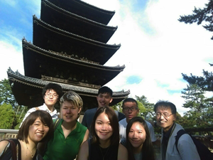
During our trip to Nagano prefecture, we did so many things, that I cant remember all of them. We left early and took the Shinkansen (bullet train) to Nagano. There, we first visited a cat shrine in the mountains. Then, we planted some rice on a family farm. After that, we soaked in the onsen at the ryokan. After eating a fancy dinner of traditional Japanese food at the ryokan, we ended our day with a Taiko performance. On Saturday, I went to the insect museum. Then, we met KIP students, went to the Shinshu University and had a discussion on the use of cellphones in classrooms. Later that afternoon, we talked to the local farmers about agriculture in the Nagano area. That evening, we had an awesome outdoor BBQ with the KIP members and some of the farmers. On Sunday, we made soda noodles and then ate them for lunch, stopped by Daihoji Temple and visited Ueda High School. There, the talented high schoolers gave us a tour of the Ueda Castle and took us downtown for some delicious local ice-cream. The trip was concluded with bus ride back to Tokyo through some really beautiful mountains.
Famous Nagano Soba and Stone Buddha Statues of Osamu
Before coming to Nagano, I have never heard of it, even though 1998 winter Olympics were held there. Therefore, I went on the trip without any particular expectations in mind. Nevertheless, it was impossible to ignore how different rural cities like Nagano and Ueda are from Tokyo. They almost seemed vacant compared to the busy Tokyo. This is because each year rural towns loose more and more people because the younger generation prefers to live in large megalopolises such as Tokyo and Osaka. The Aoki Village, where we stayed in the ryokan, reminded me of the small agriculture towns in the heart of California. Of course, there are more differences then similarities between the two. Nevertheless, both have beautiful valleys surrounded by small mountains. I was pleasantly surprised by the beauty of nature in the Nagano area. The mountains are steep, granting beautiful views to those who climb them. The slopes are full of delightfully lush greenery. I would really want to visit Nagano in winter and go skiing there.
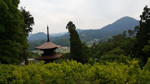
Daihoji Temple near Aokimura
During the trip, I met many different people. Perhaps, the most interesting group I got to interact with, were the young Taiko drummers. On Friday night, we went to a local Taiko dojo, where the local youths threw us an unforgettable Taiko performance. I was struck by how young and how good they were – many were elementary school aged. Many kids came to dojo right after school to practice drumming. They all, even the youngest, seemed to know exactly what they are doing with the drums. When it was NanoJapan’s time to try Taikoing, the kids paired up with the students and taught us the basic rhythms. I found the drumming very hard. However, my little sensei, who looked not older than nine, was very patient with me. Somehow, I cannot imagine myself doing the same during that age. I think this shows how Japanese kids are brought up to be studious and self-sufficient from an early age. Even though many of the kids were very shy and looked terrified of us in the beginning, by the time we had to leave, it was hard to separate them from their NanoJapan pupils. I noticed similar dynamic not just with kids, but with Japanese people in general. They can be extremely reserved, but if they open up to you, talking to them is absolutely delightful. I am already dreading the day I will have to leave Tokyo and say good bye to the KIP students.
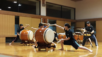
Taiko Drumming at the Aokimura The local taiko drumming troupe performing for us in Nagano.
Intro to Nanoscience Seminar
Today (Tuesday, June 2) Professor Bird gave us a very detailed lecture about the band gap of semiconductors and the basic workings of transistors. It was very helpful because I previously have not studied transistors and my project will be dealing with them. Therefore, the lecture helped me make sense of some of the articles I have read in preparation for working in my lab. On Thursday of last week, Professor Kono lectured about grapheme. Even though is not related to my research topic, I learned about many things such as Fermi energies and gates in semiconductors.
Preparation for Research Internship - Article Review
T. Yoshida, T. Tachibana, T. Maemoto, S. Sasa, and M. Inoue. "Pulsed laser deposition of ZnO grown on glass substrates for realizing high-performance thin-film transistors.", Applied Physics A 101, 4, pp 685-688, (2010). DOI: 10.1007/s00339-010-5973-9.
This article describes the characterization of ZnO thin-film transistors on glass substrates fabricated by pulsed laser deposition (PLD). Samples of varying thicknesses were tested for their electron mobility and carrier density with Hall Effect measurements. Also, atomic force microscopy (AFM) measurements determined the surface morphology and x-ray diffraction (XRD) spectroscopy determined the crystal structure of the sample. From the introduction, I found that oxide semiconductors such as ZnO can be used to create flexible and transparent electronic devices. Moreover, ZnO is an ecological and economical semiconductor. The ZnO films were first grown by PLD at high temperature of 360o C and 2 × 10⁻⁴ Torr oxygen partial pressure. Electron mobility, carrier density and sheet resistance were recorded for such films of 100 nm and 50 nm thickness. Then, ZnO films were grown at room temperature in order to apply the ZnO thin-film transistor (TFT) to an organic, heat-liable substrate. The electron transport characteristic were optimized by growing 25 nm ZnO buffer layer at 1 × 10⁻² Torr, 100 nm HfO2 dielectric high-k material as gate insulator, plus various topping layers to create a 40 um device. The result of comparing the transistors created at two different temperature shows that both ZnO films grown on heated glass substrates were c-axis oriented. ZnO channel grown at high temperature, oxygen partial pressure of 1 × 10⁻⁴ Torr and with a 100-nm-thick SiO2 gate insulator had the maximum transconductance of 5.4 mS/mm and the on/off current ratio of 1.3 × 10⁶. A TFT with a ZnO channel with buffer layer and with a 100-nm-thick HfO2 gate insulator was fabricated at room temperature. When the gate length was miniaturized to 2 μm, a transconductance of 24.1 mS/mm, an on/off current ratio of 4.4 × 10⁶ and an S.S. = 0.26 V/decade were obtained.
The Japanese tend to be very quiet when using public transportation. No one really talks out loud. Instead, everyone is on their phone. It is not uncommon to see a group of school girls huddled together as if they are going to start gossiping and giggling. But instead, each one of them is looking at her smartphone. I often catch myself wondering what are they doing: playing games, texting, web surfing?
Today, coming back home from the lab via subway, I noticed that everyone in the train car but me was absorbed in their phone. The only exception was a young man with a Gameboy. On one of the stops, a very old man came in and sat across from me. I expected him to share my abstinence from technology until he pulled out an ipad and headphones and started tapping away.
I wonder whether the Japanese are on their phone so much because talking on the train is considered rude and there’s nothing better to do. Or are they so involved in their virtual life that they are willing to forgo a conversation in favor of extra fifteen minutes online.
Like everything else in Japan, the public transportation systems are very clean. They are incredibly clean. Once, on the subway close to Shibuya, I saw a lady drop a small piece clear plastic wrapper on the floor. In US, no one would even think bending down to fetch such an insignificant piece of trash. However, her five inch stilettos did not stop her from retrieving the trash.
The incident with the lady shows that the ardor with which Japanese maintain their public spaces doesn’t just come from laws, but rather from conscientious adherence to values such as harmony. Something that seems to go against what one would typically expect from the Japanese, is the phenomenon of women doing their make up on the train. When taking the subway through the business districts of Tokyo in the morning, one can often see office ladies skillfully apply their makeup on a crowded morning train. Foundation, lipstick, eye liner, mascara and even fake lashes, are all applied on the train. Surprisingly, despite the shakiness of the train, lack of large mirror and poor lighting, the end result usually looks excellent – a business lady ready to take on a new day! This is quite unexpected of Japanese, since most people in this country self-identify as ‘shy’, and are often quite unwilling to shear personal details.
Another important rush-hour difference is the presence of ‘female only’ train car. Apparently, many female passengers are concerned about being touched inappropriately on a crowded train during rush hour. Therefore, ladies can opt to ride in a female-only car from the time when the subway opens and until about nine AM. One can also see the extent of Japanese attention to detail by examining the biking laws. For example, in many cities it is illegal to ride a bike while holding an umbrella, or to ride with both ears covered by headphones. Once can be charged a fine if caught engaging in such offences.
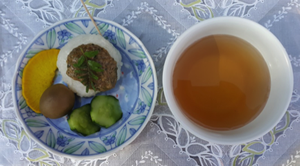
Traditional mochi prepared by farmers near Nagano
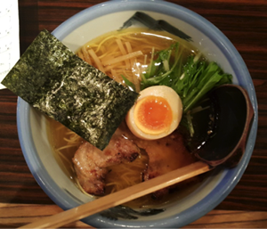
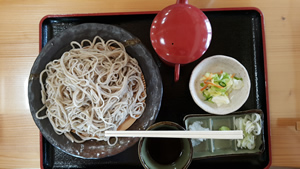
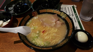
Ramen from a restaurant near Azabujuban
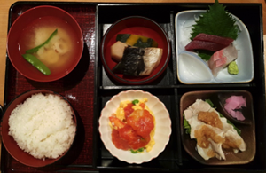
Lunch with the AJALT teachers
Intro to Nanoscience Lectures
This week’s Nano science lectures were dedicated to transistors and band structures of semiconductors.
We learned about the Moore’s law which states that number of transistors in a dense integrated circuit doubles approximately every two years. Even though it is called a ‘law’, it is actually merely on observation. The common sense tells us that the number of transistors cannot keep doubling forever because the there is a limit to how small and how close the transistors can become. In about 30 years, the transistors will reach atomic size, which is a fundamental barrier to miniaturization.
We have also learned about two fundamental approaches in nantotechnnogies: the top-down approach and the bottom-up approach. The top down approach in nanotechnology often involves modifying a bulk piece of material by various lithography and etching techniques. The bottom up approach in nanotechnology involves smaller parts coming together to form a larger whole via chemical synthesis, self-assembly or molecular assembly.
When the carrier is confined to a region where the dimensions of the material become less than 100 nm, the quantum nature of material becomes apparent. These quantum effects do not agree with the classical predictions. These quantum effects can be utilized to make new, powerful semiconductor devices. For example, the number of carriers trapped by the quantum dot can be controlled by an external voltage.
Graphene has many interesting properties that can potentially cause a revolution in the transistor industry. It has no bandgap, very high electron mobility and can carry very large current densities. However, not having a band gap means that the transistor cannot be turned off. Therefore, this kind of transistor is impossible to use. However, bandgap engineering is the process of controlling the band gap of a material by changing its chemical or structural properties. Band gap engineering can create a functional bandgap in grapheme, thereby making it possible to use in a transistor.
The lecture that explained the physics behind band gaps was the most useful to me. Not only was it on the subject that I was going to continue exploring in my lab, it also enabled me to understand why graphene is such a cool and important material in the next lecture.
My first day started off with a meeting. At 9.20 I was to report to a designated room, where the professors and students from the E and D departments were to exchange their research updates of the week. I am part of the E department. E is the electrical engineering department; however, everyone here simply refers to it as E. I am not entirely sure what D of the other department stands for, but I’ve been told that their work is similar, yet more computational. At these meetings, students usually present a power point of their recent work. The text of the power point is in English, but the delivery is in Japanese, because most students in the E and D departments do not speak much English. Before arriving, I was asked to prepare a presentation to introduce myself at the meeting. However, I unfortunately did not bring a power point because it turned out that my apartment does not have internet acess, and I could not upload any interesting pictures to my presentation. Therefore, I just talked. I first introduced myself in Japanese. Thankfully, AJALT language classes taught us how to do that very well. I was nevertheless very nervous, so my Japanese was quite broken. I hope the students could understand what I was trying to say. Then, I elaborated by self-introduction in English. Perhaps, the students could not understand much. However, all of the professor have excellent English. They asked me many questions, which put me at a relative ease.
After the meeting, the rest of my morning was free. Both Sasa-sensei and Koyama-sensei had instruction that morning. Sasa-sensei is the professor under whom I am working. Koyama-sensei is an associate professor who is more immediately in charge of my research. Sasa-sensei kindly took me to the international student center and the language learning center. Even though the language learning center is for learning English, I did manage to borrow two Japanese learning books. Then, Sasa-sensei took me to the department E office, where I remained for the rest of the morning. I found the office to be a very friendly place. Nakata-san, the secretary of department E, is incredibly nice and speaks excellent English. She offered me some Japanese sweets, and the one of the students who worked in the office made me a cup of coffee. I spent the rest of the morning drinking coffee and getting to know the students and professors of the department as they came to and from the office.
I went to get lunch with Nakata-san, and she showed me around the dining hall. To order food, you need to buy a ticket and then present it to a cafeteria employee at the counter. I got a couple of valuable insider tips from Nakata-san. For instance, to get a smaller portion of rice, one needs to bend the top right corner of the ticket. This is very useful, because the portion sizes in the dining hall are very generous. I ate lunch with Nakata-san and the secretaries form other departments. They gave me suggestions of what to visit in Osaka.
After lunch, Sun-san, a graduate student whom I will be working with, showed me around the lab. My lab consists of one very large cleanroom. This cleanroom is shared by four professors in the E department and their students. During the day, mostly graduate students work in the lab. In the evening, some fourth year undergraduates come to participate in the research. Moreover, some mornings, lab classes are held in the cleanroom. I am very lucky because Sun-san speaks very good English, and is very willing to explain things to me. He also took the effort to introduce me to many other students in the lab and the department, which I am very grateful for. Koyama-san, also speaks very excellent English. An Osaka native, he is very willing to share his immense knowledge about the Kansai region. He even gifted me with an interesting and hilarious book of the Osaka dialect. I will study hard! Sasa-sensei knows English very well. However, his voice is very quiet and it is sometimes hard to hear what he is saying. He is very nice. On Tuesday, he and Koyama-sensei took me to see Inoue-sensei – the president of the college. I was honored by all the attention I received. Inoue-sensei asked me about my background and NanoJapan. Then, he gave me useful suggestions of the places to visit during my stay in Osaka.
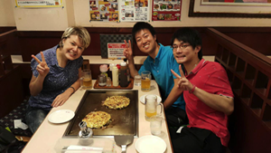
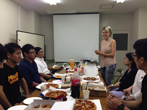
Another pleasant surprise was the Welcome and Happy Birthday Party held on Saturday. Every month or two, the E department holds a party to celebrate the recent birthdays of students and faculty in the department and to welcome new students like myself. At the party, the students cooked amazing okonomiyaki and tempura. Many brought delicious Japanese food from home. I got a cake that said, “Welcome to OIT”, which I was very touched by. I had fun time chatting with the students and the professors.
In the casual conversations, I do not feel very constrained by the language barrier. Usually, we have fun figuring out what the other is trying to say by using various dictionary apps. When it comes to talking about research, the language barrier becomes more apparent. On my project, I am working with Sun-san and Ashira-san. Mine and Ashira-san’s projects seem to be the same: making a Zn0 transistor using pulsed laser deposition. Since Sun-san is pretty busy, I have been trying to learn the pulsed laser deposition and the measurements from Ashira-san. However, Ashira-san is shy and his English is not very great, so learning has been a slow process. After the first week at the lab, my research goal is clear. However, the way I will achieve that goal is not.
I am a bit confused as to how much I should be spending in the lab. The work day here usually starts here from 9 to 9:30 (the time is pretty flexible). Koyama-san said it is alright for me to leave after five or six. However, many students stay in the lab until ten PM or later. They also work on Saturdays. On most days, I’ve stayed till about eight. My main reason for staying is acess to internet, which my apartment does not have. However, I definitely found that I learned some valuable stuff staying in the lab late. I am curious if there is any specific time NanoJapan students are expected to work per week per day or per week.
Review of the Orientation Program
I think the orientation program definitely fulfilled its goal of adapting the students to life in Japan. Not only did it do a great job teaching me Japanese and using the public transportation etc, it aslo gave me much to talk about with the people I now meet. For example, telling the Japanese about my trips to Nagano is always a great conversation starter. And talking about the many interesting things we did on those trips, such as soba-making and rice planting, usually leads to more interesting conversations. Therefore, the trip to Nagano was by far the most useful and interesting experience during the orientation.
I think everything during the orientation was quite worthwhile. Even though some of the science lectures did not directly apply to what my research project is, as a physics major, I found them very interesting and useful. As for the language learning, I will do my best to learn conversational Japanese. In my lab, there will be plenty of opportunity to practice. I think my main goal is to be able to uphold a basic conversation in Japanese.
Most important lessons from my stay in Japan so far:
-
Bathroom slipper are a THING. Do not forget to take them off as you leave the bathroom!
- Japan has a declining population and a growing number of old people.
- Japanese people are known for being reserved, especially in Tokyo. However, not everywhere is like that. Osaka people are known for being outgoing, open and hilarious! (which they are) I am lucky to be in Osaka:)
Burning question left unanswered:
Why are things in Japan are so cute and why can’t we have that in America?
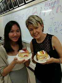
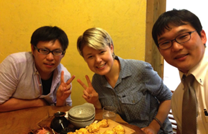
Jovia and I being welcomed as the new international students of the E department!
Dinner with labmates – first time trying Osaka specialty, okonomiyaki – delicious!
Akashiaki – a Kansai delicacy introduced to me by Koyama-sensei!
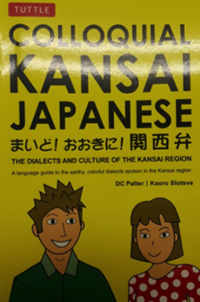
A deep and funny guide to help me navigate the language of Kansai
Research Project Overview
My main research goal for this summer is to make a ZnO transistor using pulsed laser deposition. Then, depending on how much time I have, I will make a couple more ZnO transistors in with various structural differences and see which structures yield optimal transistor characteristics. ZnO is an optically transparent material. I will have a choice of making my transistors on either glass or plastic substrate. If I make the transistors on a plastic substrate, my transistors will be both flexible and transparent. They could potentially be applied to create flexible electronics.
In order to make a transistor, I will first need to make a thin film of ZnO using pulsed laser deposition. I can vary the resistivity of my thin film by changing its thickness. I can accurately measure the resistivity and other electron transport characteristics of my thin film using the Hall Effect measurement. The thickness of the film can be determined by an instrument called Alpha Step Surface Profiler. Then, using the thin film I have made, I will need to pattern a transistor using mask photolithography. Finally, the final layers of my transistors will be created with the sputtering deposition system. In order to prepare my research project, I will need to learn to use this equipment and learn much about semiconductor physics and the structure of transistors. My plan is to finish making my first transistor by the mid-program meeting in July, and then to spend the remaining time researching ways to improve the design.
Senpai-kōhai Relatioship
Luckily, I have not had any major misunderstandings during my first five weeks in Japan. However, there are still some aspects of Japanese culture that make me uncomfortable despite of my ability to recognize them. For example, the Japanese tradition of the sempai treating his/her kōhai when eating out leaves me feeling awkward every time. On one hand, I understand that a kōhai is expected to respect and obey their senpai, and the senpai in turn must guide, protect, and teach their kōhai as best they can (according to a very helpful Wikipedia article and some common sense). Nevertheless, to me, because of my values and cultural background, being treated feels somewhat patronizing. Therefore, I cannot accept people buying me food without refusing many times first. Of course, I understand that treating one’s juniors and listening to seniors is a cultural norm here. Therefore, if senpai insists on paying, I eventually give in. However, this leaves me feeling in debt. Therefore, if I know that someone will be paying for my dinner, I want to order the cheapest thing on the menu. I wonder if it is considered very rude if I refuse my sempai to treat me. Luckily, Japanese people quite understand and they realize that I do not try to evade having the sempai pay for me because I do not recognize their authority, but rather because I grew up with different set of values.
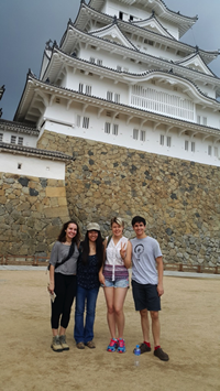
Kansai Crew Conquering the Himeji Castle\
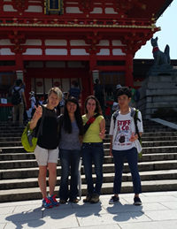
Fun day with friends in Kyoto
Put on the spot at the welcome lunch.
Research Program Update
Fabricating ZnO TFT
The past week, I was learning the fabrication process for ZnO thin film transistor (TFT). The previous week, two ZnO thin films were fabricated with different growth conditions using pulsed laser deposition (PLD) method. Both were grown with the presence of oxygen in the growth chamber. However, the first sample, 150611a, was grown at the O2 partial pressure of 11.71E-2 Torr and the second, 150611d under the O2 partial pressure of 1.94E-2 Torr. The two films were grown at the same laser power and growth time. 150611a has thickness of 40 nm and 24 kΩ while the 150611d has thickness of 41 nm and 35kΩ. Both were deposited on a glass substrate. The Hall Measurements performed last week showed a carrier mobility of 3.5 cm2/Vs and carrier concentration of 4.33E18 cm-3for 150611a and 2.75 cm2/Vs 6.70E17 cm-3 for 150611d. Also, last week I learned how to make the ohmic electrodes and channel layer using photolithography, including isolation development and etching. The plan for this week is to perform the TLM measurements for the ohmic electrodes and see if they need annealing. It is highly likely that the electrodes will need annealing. Therefore, I will learn how to do the annealing of electrodes and do the TLM measurement of the contact resistance once again. If everything goes right, I plan to add the gate insulator and the gate to the transistor by the end of this week. The HfO2 gate insulator can be deposited via the electron beam evaporation. The ohmic electrodes as well as the gate are to be made of AZO films; therefore, all of them can be deposited via PLD. So far, I am closely working with another student, who has a very similar project. We are also making a ZnO TFT under the same conditions, but with Ti and Au electrodes. We will then compare the electrical properties of the transparent TFT with AZO electrodes and the non-transparent TFT with Ti and Au electrodes to evaluate the relative effectiveness of the transparent TFT.
Biggest Personal Accomplishment:
Somehow, I managed to fall in love with my life in Osaka. This is definitely something I did not expect. I was leaving Tokyo with a sense of an impending doom. From previous experience, I know that I usually dislike a new place of residence until it grows on me a year later. Moving to Osaka was especially intimidating since I was to do it alone without anyone I know in the vicinity. Also, making friends has usually been challenging for me. So, I expected myself to be pretty lonely and miserable here. However, I managed to become good friends with my labmates despite the language barrier. And for two weekends in a row, I have been traveling with NanoJapan students, KIP students and my labmates. So, I think I have established a successful social life for myself here in Osaka.
Biggest Personal Challenge:
Learning Japanese has been a challenge. I have a fear that my knowledge of Japanese will regress by the end of the summer. I have definitely learned many new words. I can only find motivation to study the words that my labmates teach me because they are useful in my everyday life. Studying the vocabulary in the textbook, on the other hand, has been a challenge because if I cannot find an application for a new word my everyday life, I soon forget it.
Another challenge is maintaining a healthy lifestyle. There are so many things to do, that I rarely find myself sleeping more than five hours. Also, fruits and vegetables are quite expensive here, so I rarely eat them. Despite these problems with my lifestyle, I feel great and I have only been sick once since coming to Japan. However, recently I found a place that sells fairly cheap and delicious tomatoes. So, now I often eat them for lunch.
Progress with Research:
Luckily, I was able to keep up with my timeline prior to this week. However, starting this Monday, I am behind. Before leaving for Okinawa, I was supposed to finish making the thin film transistor. However, because the electron beam evaporation system is broken, I will not be able to finish making one before Wednesday. I will have to resume after Okinawa. This is of course disappointing. However, this week’s Monday and Tuesday, we will be troubleshooting the quartz crystal thickness monitor of the evaporation system, which is very exciting.
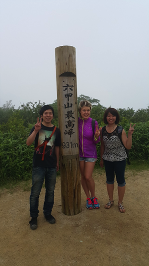
On the top of Mt Rokko!
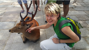
Nara’s deer
Field trip to Nara with a tour by Kimura-sensei of the wonderful E-department
Research Project Update
Past week, I performed transmission line method (TLM) measurements for the ohmic electrodes of the transistor I am making. I determined that the electrodes require annealing because their resistance is too high. Therefore, I performed annealing on the transistor samples and then checked them again with TLM. The annealing was done at 400 degrees C. This time, the resistance was lower and the IV characteristics of the transistor were improved. The next step was to deposit the HfO2 gate insulator. Therefore, I patterned the gate onto the TFT using photolithography. The next step would have been to deposit the HfO2 onto the coated film using electron beam evaporation (EBE). However, the EBE appears to be broken. Particularly, the spring in the quartz crystal oscillator of the EBE appears to not function correctly. Therefore, the rate of deposition cannot be measured correctly. This is concerning because in order to deposit a film of the right thickness, we need to know the deposition rate. Therefore, the remainder of the week was spent troubleshooting the EBE. So far, results are inconclusive. My plan was to make the ZnO TFT before the mid-program meeting in Okinawa. However, now the TFT needs to be finished after my return from Okinawa. At this point, Koyama-sensei will call the company of EBE and request their help in fixing the system.
Learning Japanese is one of the biggest challenges of living in Japan for me. At the end of the orientation program, my level of Japanese was high enough for me to give a decent self-introduction, to sound polite and to make purchases. Unfortunately, my Japanese is still not good enough to have a satisfactory conversation. Usually, any attempt to extend a conversation beyond the basics of my self-introduction results in either becoming a completely dependent on a dictionary app or gradually turns into English. However, the self-introduction words and courtesy expressions that we learned during the orientation are very useful. When I arrived in Osaka, I was meeting many new people and I always introduced myself in Japanese. I think this made a good impression on people and perhaps made me more approachable.
I have not had a language experience that stands out as extraordinarily difficult. As of yet, I have not had any major miscommunications or instances of being lost because of not knowing Japanese well enough. I am not too worried about running into a situation where I get in trouble due to my poor language skills because I am lucky to have free mobile data on my phone anywhere I go. So, I know if I run into a problem, I will likely be able to resolve it by translating what I want to say and what I am told. So far, the most difficult aspect of learning Japanese has been to consistently keep studying it everyday. Some days, it is hard to find time and/or motivation to review or memorize new words.
So far, the most effective way of learning Japanese has been simply memorizing vocabulary and then either trying to integrate them into my speech or listening for them in the conversations of others. A fun way of learning Japanese that I have recently discovered, is translating comic books. During the Mid-Program meeting, I have seen some fellow NanoJapaners translating Japanese children’s books into English. I thought it was a great idea. So, after returning to Osaka, I’ve acquired some manga and so far I have really enjoyed translating it. I think I will continue to translate Japanese comics after my return to US as a hobby. I will also try doing the same for Chinese.
During the mid-program meeting I discovered that I am not as behind in my project as I have thought and that many of the students are at a similar stage in their progress. I also discovered that many students ran into similar problems in their labs as I did and it was very helpful to talk to them about it. For example, one of the students mentioned feeling like her lab did not expect her to do much work. I have definitely felt that when I first arrived at my laboratory. For example, I was told I can leave at five even though in reality, most research in my lab starts after six when students return from class. I had to show my lab mates that I am very willing to work hard by being active: staying in the lab until everyone leaves, asking many questions, and asking students to show me how things work. It was interesting to find out that some other students had similar experience.
In Okinawa, I really enjoyed getting to know other students who attended the MTSA conference. There were both Japanese students, as well as students who flew in from abroad. It was very interesting talking to them about their research and graduate student life at their universities. I also really enjoyed the lab visits. OIST has extremely nice facilities. I think of this university as of a research paradise. It is graduate university with a very progressive vision. I love the idea of interdisciplinary research and the rotation system for new students. I would definitely like to apply there for graduate school. However, there is just one problem that makes OIST a bit less attractive: it quite far from any major cities. I think living there one might feel isolated.
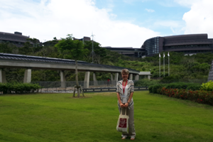
OIST is a research paradise
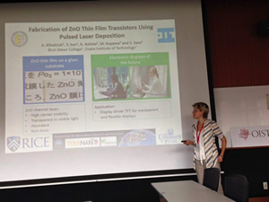
My presentation at the student session of the MTSA
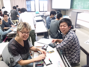
I've been invited to attend one of the ‘active learning’ lecture classes at OIT, where I got to explore the current-voltage characteristics of a solar cell.
Research Project Update
Three pieces of equipment that I am supposed to use for my project broke. The electron beam evaporation that I was supposed to use for deposition of HfO2 was unused for a very long time and therefore had an uneven deposition rate as shown by the machine. This made it impossible to determine how long the deposition should be in order to get the desired thickness. On Monday, we deposited a HfO thin film in order to try to figure out the deposition rate. However, when as we were measuring the thickness of the HfO2, Alpha-Step, the equipment that measures thickness stopped functioning. On Tuesday, we were cleaning the cooling system of the electron beam evaporation because the water pipes were partially clogged which might have led to the overheating of chamber and uneven deposition rate. This week, a person from a company will come to fix the Alpha step. On Friday, someone damaged the pulsed laser deposition. The problem was fixed. However, the vacuum inside the main chamber was broken and now the chamber needs to be baked in order to get rid of any moisture. Because of these mishaps, I am now behind my schedule by about a week. Hopefully, I can finish fabricating my fist TFT by the end of this week.
People’s interactions in my lab are mostly governed by the lab hierarchy. However, the hierarchy is not as strict as I thought after the attending the orientation program and hearing the stories of my alumni mentors. The hierarchy is most clear from the way undergraduate students, who come to work in the lab after class, treat their graduate sempai. The undergraduate seniors quietly and respectfully tip-toe around the lab, and watch attentively what the graduate students are doing and do exactly as they are told. The undergraduate students agree with everything grad students say and do. Also, the undergrads can’t ask the grad students to do anything for them.
There was in interesting episode where one of the undergraduates forgot his laptop in the cleanroom. Going back to fetch it takes quite a bit of effort because to enter the cleanroom, one needs to put on the cleanwear. I suggested that he should just ask someone to bring it out of the cleanroom for him. But he said it can’t be done because everyone in the cleanroom is his senior.
There seems to be a lesser divide between the graduate students of different levels. They all seem to be very good friends. They can argue and address each other informally with –kun. Everybody else usually just addresses each other as –san. Sometimes, the doctorate student in the lab gets addressed as –sempai. And the assistant professor, who does research with the students in the lab, is respectfully addressed as –sensei. No one challenges the authority of the professor or the doctorate student.
It is hard to compare my Japanese lab to my lab in US because they are too different. I worked in spintronics lab in US, which mostly does physics and a lot of basic research. While here in Japan, I work in nanodevices laboratory and most research here is very applied. In my Japanese laboratory, most students are pursuing a master degree with the intent to enter the workforce afterward. However, back in US, most students in my lab were PHDs with the intent to enter academia. I think that the master students in my Japanese laboratory are most focused on gaining research experience that will be useful for them when they work in the industry. They are doing research that will hopefully make them more competitive during their job search. They seem to be quite focused at becoming really good at the fabrication technique they are studying. In US, the students are very focused on publishing papers.
I think I actually really like the nanodevice laboratory here in Osaka Tech. It is much bigger then my laboratory in Bryn Mawr and is very well run. Everything is very conveniently organized. My laboratory in United States is very small and does not have such a sophisticated level of organization and resources. I am getting better mentorship here than in the States. However, I do really miss the autonomy I had in the Bryn Mawr with my research. There, I was learning much quicker because I was doing everything by myself. Here, however, the undergrads are not expected to do much in the cleanroom other than perform very basic measurements and watch the grad students work.
Therefore, I can only work on my project with some graduate student helping me out. It is reasonable, since most of the equipment I am using are very expensive, sensitive and complicated to use. I really don’t want to break them, but at the same time I wish I could work alone. Because right now, I need to wait a lot for the graduate students to come back from classes, part time jobs etc so that they can help me. So, being a visiting undergraduate in this laboratory is not so great. However, being a graduate student here must be really nice.
Ichiran, the most amazing ramen I’ve had so far!
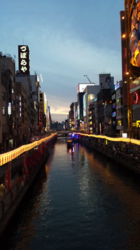
Dusk in Dotonburi, Osaka
Research Project Update
On Monday and Tuesday, the electron beam evaporation system remained dysfunctional until we replaced the quartz crystal microbalance on Wednesday. The microbalance is responsible for the measuring the growth rate of the film during deposition. Previously, the instruments showed the growth rate to be very unstable, so we could not deposit the film. It is possible that the microbalance was damaged when the cooling system was working poorly. After the microbalance was replaced, the instruments showed stable growth rate and we could finally deposit the HfO2 gate insulator layer on Thursday. At the same time, we deposited two more ZnO thin films for the next transistor. On Friday, we performed Van der Pauw Hall measurements for the films to determine their resistance.
The plan for this week is to do photolithography for the gate electrode on Monday and deposit the electrode on Tuesday. Then, test the electronic properties of the transistor. At the same time, I need to start making the second transistor. Hopefully, I can deposit the channel layer and the ohmic electrodes this week.
I interviewed Koyama sensei, an assistant professor and a senior researcher in my lab. He has a PHD in semiconductor engineering. His decision to pursue a PhD in this field was strongly influenced by his fascination with solid state as well as quantum physics. He was inspired by Dr. Inoue, who was his electronics professor at Osaka Tech during undergraduate years, and became his research mentor in graduate school. Professor Inoue encouraged Koyama-sensei to pursue a PhD because he saw a he has a potential to become a researcher. In graduate school, Koyama sensei was studying ballistic nanodevices. After completing his PhD at Osaka Tech, Koyama-sensei worked as a researcher at a company for a number of years. At the company, he was developing high mobility transistors for gallium nitride and aluminum gallium nitride heterostructures.
His reflection on the job search process and the differences between researching at the university vs. in the industry are as follow: It is very difficult to find a job at a company for a person with PhD because the doctorate students have greater theoretical knowledge, while the companies are looking for people to do applied research. Moreover, the aims of research done at a company and a university are often quite different. At a university, the focus is on inventing an original device, while the companies’ research often focuses on how to mass produce something at a low cost. After working at the same company for five years, Koyama sensei left his job and became an assistant professor at Osaka Institute of Technology where he completed all of his degrees some years prior. He likes the freedom to choose his own research topics that comes with his research position. However, there are the typical stresses of being a researcher: need to publish papers, apply for grants and teach classes. When Koyama-sensei becomes a tenured professor, he hopes to establish research exchanges with the local tech companies where some of the university’s graduate students will be able to gain experience of working in an industry, while the companies will benefit from their expertise and energy. Even though my laboratory does not have any international students except for myself, Koyama sensei said that normally there are at least two international students visiting per year. Also, they are trying to send their graduate students to study abroad at laboratories of collaborators. Koyama-sensei himself hopes to be able to do research aboard in Austria for some time in the future. As the main differences between researches in abroad and in Japan, he identified the hierarchical system which constrains many of the labs. He thinks stringent hierarchy hampers creativity and that research can be done productively in a more casual environment.
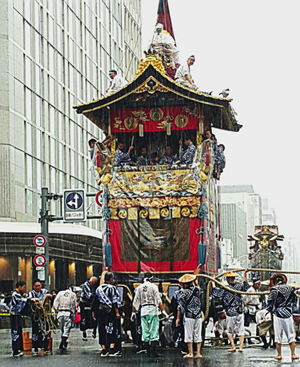
Rainy Gion Matrsuri
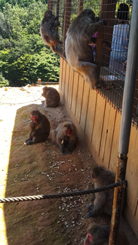
Humans in cage and monkeys outside.
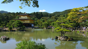
Kinkakuji did not disappoint. Looks as nice as advertised!
Research Project Update
Last week, I have completed the necessary photolithography steps for all four of my initial samples. I then deposited Au and Ti gate layer on the two non-transparent samples and AZO gate layer on the two transparent samples. This step took a long time because during my first try, the TiAu layer was overdeveloped and the gate electrodes were damaged on multiple samples. Therefore, I had to completely remove the AuTi electrode by soaking the sample in phosphoric acid and then redo the photolithography and deposition for the gate electrode.
I also deposited the channel ZnO layer using PLD for onto the four samples of the second batch. Now that my fist set of TFTs is complete, I need to make a second set with different parameters in order to compare the characteristics of the two. This week, I have already deposited the ZnO channel layer for these samples using PLD and did the photolithography for the ohmic electrode layer. By the end of this week, I am hoping to make the gate insulator layer. Luckily, the fabrication process for the second set of TFTs goes much faster than for the first. This is because, now that I have been shown how to make the first one, I can make the second one myself, without being too reliant on my labmates. Nevertheless, I am worried about running out of time.
Also, this week, I will measure the electrical properties of the transistors I have fabricated and find out if they actually work. I will use TLM measurement process and Semiconductor Parameter Analyzer to do so. Keeping my fingers crossed!
After reading about Obokata’s controversy, I was disappointed with Obokata since she behaved unprofessionally and most likely fabricated her research when the media played so much attention to her. However, I do think it is fair that she got a chance to prove that her results can be replicated. I sincerely hope she does prove herself right. Otherwise it will further hurt the image of women in science in Japan.
I think the media was largely well-meaning in all of the attention that it paid to Obokata when she was coming up with the stellar findings. Of course, the media did treat Obokata as a ‘panda in the zoo’ because media always looks for something sensational. Nevertheless, the media attention would have helped prove to the Japanese that female researchers are just as good as male researchers. I am not sure whether Obokata’s flamboyant style would have helped or hampered the female scientists if her research proved to be viable. I think she might have overstepped some boundaries and drew more media attention to herself then necessary. This worsened the impact of her fabricated results. I am puzzled at why Obokata was drawing more attention to herself when she knew that her research was not genuine. I think this might have happened because perhaps she was one of the very few women researchers in her workplace. Thereby, perhaps she was faced with different expectations then the male researchers in her company. Therefore, it was easy for her to act unprofessionally such s not keeping good record of her research, not wearing a lab coat etc.
Since I am the only female in my laboratory, it is difficult for me to make any conclusions about the treatment of female scientists in Japan from personal experience. I am treated very courteously and respectfully in my lab. However, I think this is due to the fact that I am a foreigner. Whenever I complete some step of my research on my own, everyone seems to be extremely impressed with me. I tend to attribute such low expectations to the fact that I am an undergraduate student. Since I go to an all-women’s college in United States, it is once again very difficult for me to make any conclusion about the difference in treatment of male vs. female researchers in America. In the United States, I was faced with very high expectations, despite being an undergraduate in my lab. I definitely did not receive any special treatment, as I do in Japan. However, I was always treated fairly and equally.
The overall gender issues in Japan are a bit more apparent. One of the clearest examples is the obvious lack of female students at OIT. Walking though campus, I see that almost every student here is male. Clearly, it is not very common for females to pursue tech degrees and go to a polytechnic university. Moreover, I haven’t encountered any female professors here either. There are more such examples. The all-female train cars, all-female hotel floors, etc. Having such special conveniences just for women is nice, but not very equal.
Research Project Update
At the beginning of this week I finally completed fabricating the second set of transistors. However, I have not yet had a chance to measure their electrical properties. However, it is possible that most of these transistors will not work. This is because we decided to use a longer development time for the second set of samples, since for the first set, the development time was too short. However, in the second set, the channel layer got partially removed along with the photoresist. This week, I started analyzing data from the transistors in the first set.
Attitudes toward Japan: Initially, my understanding of Japan was based on 1) anime and drama, 2) history class, 3) stories of people who lived there. Before arrival in Tokyo, my expectations of Japan was very vague. After two months of living in Japan, these are my strongest impressions.
Attitudes toward United States: Living in Japan made me realize just how rude most people are in America. Living in the US, I was never really concerned with impoliteness. I always thought, “this is just how things are”. However, seeing how considerate and kind Japanese are toward each other every day, I now realize that it can be different. Therefore, getting yelled at in the Houston airport was more upsetting than usual.
On the bright side, having trashcans around is a joy.
Personal Impact: Spending a summer studying and living in Japan had a big impact on my personality. A mix of freedom, relaxed expectations and desire to experience and see as much as possible, left me a little bit of a different person.
Firstly, I became much more confident in my social skills. During these two months, I’ve met more new people then I’ve met in the last two years. Therefore, I got better at turning strangers into friends.
I became much more confident in myself in general. This summer, I’ve traveled alone a lot. While, traveling, one is always faced with many unexpected situations. Successfully resolving such problems made me feel more prepared for life.
I became more outgoing and actively started trying new things. As result, I am now much more comfortable with putting myself in potentially uncomfortable situations.
I am trying to be more polite and considerate towards others.
Daily Frustrations: Buying something wrong, or not buying something because I could not read the label. Lesson learned: need to take language study more seriously.
What will you miss the most? I will miss my friends and lab mates, as well as the variety of drinks.
Impact on research and career goals: This summer experience definitely gave me more to think about regarding my future. I confirmed that nanodevice engineering is indeed a very interesting field. It is not a candidate for what I can study in graduate school. Furthermore, I am now considering the possibility of going to graduate school and/or working in Japan.
![]()
The main goal of my project was to fabricate and characterize transparent ZnO-based thin film transistors (TFTs). Most of the thin film layers of the transistor were to be deposited via pulsed laser deposition (PLD). I fabricated two sets of TFTs intending to compare their electronic characteristics and find the optimal deposition procedure. The two sets were different in that the first set had the gate insulator fabricated via the electron beam evaporation EBE and the second had the gate insulator fabricated with PLD. Each set had four samples: two with Ti/Au electrodes and two with AZO electrodes. AZO samples were completely transparent, however, their characteristics were difficult to measure because of high contact resistance. Ti/Au samples have very similar characteristics, yet, easier to measure. However, due to problems within the deposition process, only the transistors with Ti/Au electrodes and gate insulator deposited by EBE worked. Transistors with gate insulator deposited by PLD were broken because PLD had a problem depositing HfO2, which is the material used for gate insulator. Perhaps, this happened because the intensity of laser did not match the energy level neede to excite HfO2 and cause its ablation. Likewise, the transistors with the AZO electrodes and EBE deposited gate insulator did not work because the gate insulator was dissolved due to overdevelopment of photoresist. Therefore, I was only able to measure the electrical properties of transistors with Ti/Au electrodes and gate insulator deoposited by PLD. I used transmission line measurement method and semiconductor analyzer to test the transport and output characteristics of TFTs. These TFTs were measured to have a transconductance of 2.6 mS/mm and an on/off ratio of 1.3X10. A functional ZnO TFT with Ti/Au electrodes was obtained with using PLD to grow channel layer, Ohmic electrodes and gate electrodes, as well as EBE to grow the gate insulator. Further investigation needs to be done to optimize the deposition conditions of PLD and determine the fabrication process for ZnO TFTs with gate insulator grown by PLD and for ZnO TFTs with AZO electrodes. Transparent TFTs were fabricated without the use of rare earth metals creating a relatively cheap and non-toxic transistors.
When speaking to a family member, I would say the most important thing I learned from Nanojapan is confidence. At the beginning of the program, we have been told that as international students in Japan, we play an important role as American cultural ambassadors. Therefore, while in Japan, I did my best to act with American confidence and directness. This was reflected in almost everything I did from asking for directions on the street, to giving presentations at lab meetings, to operating complex lab equipment on my own. Over time, I noticed that it was easier for me to spontaneously enter a conversation, try something new, or ask for help from sensei. Being an undergraduate in my lab, I knew much less then my graduate labmates. Being a foreigner, my ability to communicate was also limited. However, I learned to be confident in my abilities, even while knowing that my knowledge and skills are not perfect.
If speaking to a professor, I would discuss how NanoJapan has furthered my knowledge of physics and electrical engineering. Working in a graduate-level laboratory and interacting with my labmates gave me a good idea of what it means to be a researcher working on nanodevice fabrication. Not only did I learn many useful lab skills such TLM and Hall Effect measurements, photolithography and using AFM, but also learned how I can apply physics to electrical engineering and nanotechnology research. This gave me a better idea of what sort of research I want to do in the future. I now know what books I want to read and what classes I should take to pursue my academic interests.
If speaking to an employer, I would talk about how Nanojapan has taught me cross-cultural communication. Even when speaking English, my communication with the Japanese people was very different from my communication with Americans. This is because Japanese people have different cultural values and expectations and customs. I learned to interpret ambiguous ‘maybes’, gracefully accept being treated, see kindness in formal polite expressions. I had to adapt my own communication style as to keep my confidence and directness, yet not seem impolite nor too demanding to Japanese people. I learned to work effectively in a cultural environment different from my own.
When speaking with a fellow student, I would say that Nanojapan taught me how to not only survive in a foreign country on my own, but also enjoy my life there. I learned how to be adaptable by having to adjust my schedule to the one very different from my usual school routine. While in Osaka, I spent an hour every day to travel to school by subway, had access to internet only while in the lab, ate dinner after leaving lab at 11 pm and used cash for all purchases. I discovered that I love trying new things and finding new experiences. In Japan, there were so many things I’ve never seen, heard of or tried before. I wanted to learn about all of them and I only had eleven weeks to do so. Therefore, I did my best to always travel to new places, eat new foods and seek new experiences. As result, I returned to United States being a more open-minded, adventurous and accepting person.
Living and working in Japan this summer has fundamentally changed how I think about Japan, study abroad, and the possibility of living in a foreign country. For instance, after coming back from Japan, I decided to rewatch an old anime I used to watch few years ago and discovered an entirely new dimension to it. Many characters and scenes that seemed trivial suddenly found new significance and the message of the animation now seems different. My interest in Japan is as strong as ever, however I noticed that while previously I was more interested in Japanese contemporary culture such as fashion, anime, and j-pop, I am now more interested in the traditional aspects of culture such as literature, history, politics, philosophy. While before I thought that one study abroad experience will be enough for me, now I am determined to do research abroad next summer as well. This is because I realized that merely traveling abroad does not produce the same effect as studying or working abroad. By studying or working in a foreign country, I can experience the everyday life there as well as gain a deeper understanding of the culture and values. While, previously I have not seriously considered studying or living abroad for an extended period of time, I now am seriously considering applying to graduate schools abroad.
After returning from Japan, I still have many questions left unanswered. My top two are:
One day, I hope to return to Japan to look for the answers to these and many more questions.
My summer with NanoJapan was incredibly meaningful and unforgettable. Thank you so much to everyone who made it possible!