Alumni Update & Further Accomplishments
| Barry M. Goldwater Scholarship >> Website |
|
 |
Ethan Schaler - NanoJapan 2008 2009 Goldwater Scholarship Recipient As a recipient of the Goldwater Scholarship Ethan will receives a two-year scholarship that will cover the cost of tuition, fees, books and room and board toward her undergraduate studies at the University of Maryland, College Park. Ethan states, "I based a large amount of my application on my research in Japan - especially at RIKEN - and my research proposal essay in particular was a combination of work that I performed at RIKEN and UMD. For this reason, I wanted to let you know of the outcome and thank you all for helping me have such a great opportunity to do research in Japan!" >> Student Profile |
| RIKEN - NanoJapan Alumni Program >> Website |
|
 |
Ethan Schaler (NJ 2008) will return to RIKEN in the summer of 2009 to conduct research in the NanoPhotonics Laboratory under the advisement of Prof. Kawata and his research mentors Norihiko Hayazawa, Alvarado Tarun, and Masashi Motohashi. He will be in Japan from June 20 - August 27, 2009. >> Student Profile |
 |
Bridging Scholarship for Undergraduate Study in Japan >> Website |
|
Ethan Schaler (NJ 2008) has recently been awarded a Bridging Scholarship for Study in Japan to participate in the Tohoku University JYPE (Junior Year Program in English) through the Global E3 Program. He will study there from September 2009 through February 2010 and in addition to coursework will also be conducting research with Dr. Hiroki Kuwano in the Micro/ Nano-Machining Center. >> Student Profile |
NanoJapan Research Overview
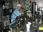
I conducted my research at the RIKEN government research institute in the Nanophotonics Laboratory, which turned out to be a truly extraordinary experience. My investigation focused on the measurement and 3D parameterization of internal strain at sub-micrometer resolution using a novel far-field Raman spectroscopy technique proposed by my mentors. I constructed the optical equipment array necessary for the imaging technique, observed strained silicon wafer samples, and processed the data using programs developed by my mentors and myself. Work in an international government research laboratory was a very interesting experience: a large majority of the Japanese scientists spoke English (making communication very easy), and everyone was eager to both learn about / provide input on the work I was conducting and demonstrate the research that they were working on.
I plan to maintain my engineering studies through graduate school in order to continue to expand both my technical knowledge and research capacity in MEMS design and fabrication. I aspire to then pursue international and interdisciplinary research in this same field of nanotechnology. As a result, the research I conducted at RIKEN provided a critical introduction to nano-scale 3D fabrication and optical observation techniques that will be beneficial to my future research. I also (now) hope to conduct this research at an international institute where I can collaborate with scientists from across the globe while simultaneously exploring a foreign country.
Meaning of NanoJapan
I personally selected the NanoJapan program due to its unique balance of novel research in premier Japanese institutes with immersive exposure to Japanese culture and society. This experience surpassed all possible expectations I had for my very first international trip, and built the foundation for a true cultural awareness and interest in pursuing international research collaborations – a necessity in an increasingly interconnected world.
The first aspect of my NanoJapan ‘experience’ was the ability to conduct research in a cutting-edge international scientific laboratory with some of the premier Japanese nanotechnology experts. Kawata-sensei is a world-renowned professor in the field of nanophotonics who heads departments at RIKEN (the government laboratory where I worked) and Osaka University, has been presented with numerous national awards for his achievements, and even controls a company that produces nano-optical devices for various experiments. My personal research interests lie primarily in the design and manufacture of MEMS (micro-electromechanical systems), so the research that I conducted at RIKEN – using an optical microscope to measure nano-scale strain within a silicon sample – is a perfect prelude to more intensive design and imaging of these micro-scale devices. I’m also sure that the connections I’ve made with other scientists through this work will continue to benefit me in the form of future research collaborations.
The second aspect of my NanoJapan ‘experience’ was the ability to acquire a knowledge and intimate appreciation of foreign cultures through first-hand experiences. My long chats with a few close Japanese friends provided depth to my understanding of Japanese society and the experience of growing up there. My conversations in mixed Japense-English with complete strangers (lasting from 5 minutes to over 2 hours), which I had when traveling to numerous Japanese cities and meeting Japanese citizens on my own, were also a completely new and liberating experience that revealed even more about the world I was in. Even now, I try to stay abreast of current events and some small degree of the pop-culture in Japan (I’m also proud to say that I’m now an advocate of various Japanese bands and love the clothing styles in Tokyo). My personal experiences there were so momentous that I’ve elected to continue my study of Japanese at UMD and plan to return to Japan both next summer and for extended periods of time in the future.
Daily Life in Japan
I had a truly excellent experience working at RIKEN throughout the summer. My life there was always packed to the brim with a plethora of activities related to my research, language study, and exploration. Regarding my living arrangements, I was given extremely nice housing located directly on the RIKEN campus. The apartment was quite amazing (especially given my dorm back at UMD). I had a private bathroom and shower, a dining room with a complete kitchen (stove, sink, pots/pans, refrigerator, rice cooker, water heater, and toaster), and a bedroom. My greatest pitfall and achievement in my own home was probably taking over a month to understand that a small thermostat-looking device did not actually control the room temperature but was in fact responsible for my frigid 25ºC showers every morning. All in all, however, I couldn't have asked for anything else in my apartment, and was quite comfortable and capable of cooking / taking care of myself.
My apartment was also perfectly situated. My commute to work took about 3 minutes (by foot) and could not have been more convenient. The campus was also located about 20-30 minutes (by foot) or 5-10 minutes (by bike) from downtown Wako and the subway (with another 20 minutes to travel into Tokyo). There is also a gym and supermarket (where I was able to find more than enough food to cook healthy meals for myself – even as a vegetarian!) within 5 minutes of the campus. I was also fortunate enough to borrow a bicycle by my mentor, which gave me a great deal of freedom for exploring the local town and traveling into Tokyo (it’s also the first time I saw a ‘double-decker’ bicycle parking lot).
Regarding my daily routine, weekdays were spent conducting research and Japanese language classes (provided for free at RIKEN no less) while weekends were spent exploring Wako, downtown Tokyo, and other cities in Japan. A typical day involved me getting up around 7:30 for a brief run and breakfast, report writing / editing and data analysis work from 9-12, lunch with the entire lab from 12-1, experimentation in the lab with my mentors from 1 to 5-7, and then back home to buy food, cook dinner, catch up on work and Japanese, say hi to my family over Skype, and watch Japanese TV / News before bed. I never encountered problems with a language barrier between myself and other scientists in my lab, and so I often relished the challenge of finding new places to visit on weekends (be it museums, parks, national monuments, or isolated mountain resort towns) that were off the beaten trail and typically visited only by Japanese people.
My favorite experience in Japan was...
I was an extraordinarily prodigious traveler and was fortunate to experience many amazing and beautiful sights across Japan. It’s truly impossible for me to encapsulate the sheer diversity of lucky breaks, chance encounters, and breath-taking experiences (even the 9,000 photos and videos I took on the trip fail to capture every last joyous moment) – but I’ll do my best to highlight a few.
I’ll leave the rest of the events to be shown in my photos on the NanoJapan 2008 photo slideshow but all I can recommend is this: Travel As Much As Humanly Possible! Buy a Japan Rail Pass and just go crazy for a few weekends! There’s too much to see across Japan and you’ll definitely appreciate it as much as I did.
While I was in Japan I wish I had...
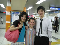
Had the opportunity to spend more time with my “Nihon no tomodachi” (Japanese friends). I met several fascinating individuals – two in particular being Tamagawa Eri and Yang Yulong – through the student discussions that were organized during the three-week orientation between NanoJapan students and students from the University of Tokyo, Keio University, and other local universities. The discussions allowed me to gain an appreciation and view of unique cultural perspectives held by Japanese students my own age and who were as interested in American society as I was in Japanese society. The dinners and more informal discussions that often followed these meetings were some of the highlights of my orientation in Japan and the subsequent occasions that I met up with Eri and Yang during the summer were some of the most enjoyable evenings I had. All the same, I’d have loved to meet up with them more often and have the chance to see sights that only a native of Japan would know about (visits to hole-in-the-wall restaurants, movie theaters, and a Japanese Shakespeare play were just a few of the fun things I did with them). Fortunately, I’ve remained in touch even after returning to the US and hope to see them when I return to Japan in the future.