Jaret Lee - NanoJapan 2006 Int'l Research Experience
Rice University
AIST: Research Center for Advanced Carbon Materials
Advisors: Kazu Suenaga and Dr. Sumio Iijima
Project: High Resolution Electron Microscopy of Er@C-90 in Peapods
B.S. Electrical Engineering, Rice University (2008)
M.S. Electrical Engineering, University of California, Santa Barbara (2010)
Current Position: Ph.D Student, Electronic Materials Engineering, Australian National University, Expected 2013
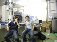
Jaret Lee (l) with lab group member at AIST
NanoJapan Overview
As a current graduate student working in the area of nanotechnology, I would like to give credit to the NanoJapan Program for helping shape who I am today. The program has fueled me with desire and passion to further explore the area of nanoscience and nanotechnology ever since. It was a very unique experience to be able to work with established scientists at the National Institute of Advanced Industrial Science and Technology, one of Japan’s most prestigious research entities at an early age. I was very lucky to have worked with Dr. Sumio Iijima, who first discovered carbon nanotubes using transmission electron microscopy (TEM) in 1991, and Dr. Kazu Suenaga, who is an expert in TEM and carbon characterization. My 2006 research project was on in-situ characterization of Erbium C-90 endohedral metallofullerene molecules using TEM. These molecules were encapsulated in single-walled carbon nanotubes (SWNTs) for TEM observation. We found that SWNTs not only serve as ideal nano-scale sample holders for directly imaging the molecular structure, but also from the material perspective, these encapsulated molecules can change the electronic structure of SWNTs thereby providing a means for on-site bandgap engineering. In addition, we investigated the dipole ordering of these molecules in these SWNT-confined cages. In the end, we were able to estimate the critical diameter for encapsulating these molecules inside SWNTs. Overall I was very satisfied with what I accomplished during the seven-week research internship.
During this time, I also managed to have plenty of fun outside of the lab with other NanoJapan participants. Some of my favorite weekend activities include shopping in Shibuya, enjoying the Japanese hot springs in Hakone, and fishing at the Izu Peninsula.
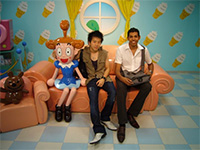
Jaret Lee (l) with fellow NanoJapan Participant Jason Holden
Before I left for Japan I wish I had...
I wish I had a better command of the Japanese language. Even as a native of Taiwan and knowing many kanji (Chinese characters), I still found it difficult to communicate with others without knowing more vocabulary. Although the language program in the beginning was very helpful, once the research program started I found myself busy doing research and lacked the time to devote to Japanese learning. For future participants, I would strongly recommend picking up Hiragana and Katagana before your arrival in Japan. If you do this you will be able to use your time in japan to strengthen your knowledge of Japanese as you will constantly exposed to the spoken language while you are there rather than spending time trying to memorize these alphabets.
Jaret Lee - NanoJapan 2009 Alumni Internship
Internship Host: STS Elionoix
Project: Research for new application of patterning by electron beam lithography; Double-coated resist process optimization using ELS-7500 and ELS-7500EX electron beam lithographic system
![]()
Internship Project Abstract
STS Elionix is a world-leading manufacturer of electron beam lithographic systems. The internship program focused on the training of ELS-7500 and ELS-7500EX electron beam lithographic system and involved the process optimization of double-coated resist for lift-off utilizing ZEP520A and PMGI resists. The goal was to create an T-shape resist patterns in one single e-beam exposure. The desired feature is made up by an 80nm ZEP520A layer on top of a 50 nm PMGI layer. The top-layer window has a 50 nm line-width, and the pitch size between successive patterns is 100 nm. At the end of the program, not only did I achieve the proposed goal, but I successfully shrank the overlying window to 15 nm line-width. More importantly, I became proficient in ELS-7500 and ELS 7500EX operation and gained practical knowledge about lift-off processing.
I am indebted to a large number of people for my successful internship at Elionix. First, I should thank Mr. Ken Koseki, Mr. Yusuke Uchiyama, and Mr. Cho Yong-Hyun at Elionix Inc. for organizing this internship and assisting me when I needed help. I am also thankful to Professor Junichiro Kono of Rice University, USA, and Ms Sarah Phillips and Ms. Keiko Packard of Rice NanoJapan Program, who gave me the opportunity to participate in this international internship. Finally, I wish to express my hearty thanks to KAUST management for their financial support in making my participation possible.