Alumni Update - Michael Chien Awarded 2009 Sigma Xi Superior Poster Presentation Award
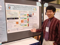
At the Sigma Xi: Scientific Research Society's 2009 Annual Meeting Michael Chien received a "Superior Presentation" award for a presentation he gave on his NanoJapan 2009 resaerch project: "Manipulation of Nanostructures on Silicon (111) 7x7 Surface for Applications in Quantum Computing".
>> Watch a Video of Michael's Poster Presentation
Why NanoJapan?
If you’re like me, figuring out what to do over the summer is always a chore. While wading knee-deep through exams, papers, and presentations, nothing ever seems quite right, and there is always the sense of foreboding that you might have to spend the summer cleaning test tubes. However, as soon as I read about the NanoJapan program, I knew that it would be the perfect summer. With my varied interests, it’s difficult to find something that satisfies both my scientific interests as well as my cultural ones. NanoJapan will do both. I have never conducted research in a lab before, so I am looking forward to the experience of working with Professor Itoh and his colleagues. My hope is to learn more about the techniques and lifestyle of physics research, which I am considering in the future. Additionally, Japan is high on my list of countries yet-to-be-visited. From sampling the local fare, to trying to speak and read Japanese, or just exploring Tokyo with my camera in hand, this summer promises to be eventful and educational, both in and out of the lab.
Studying in the United States is both an advantage and a handicap. Being advanced in many fields means that most of the time, people come to us, and even when they don’t, they still speak English. I think one of the best aspects of the NanoJapan program is that it will force me to leave my comfort zone, to immerse myself in an unfamiliar place, and more importantly to learn to collaborate with people who don’t speak my language. Japan is at the forefront of nanotechnology and applied physics research, being heavily involved in areas such as silicon fabrication for applications in quantum computing (Professor Itoh’s lab being an example). International collaboration will be essential to succeed in this field, and even if nanotechnology does not end up being my exact career, simply just stepping outside of our monolingual bubble will have been a worthwhile experience. In the future, I definitely plan to continue to be active in international research collaborations. While I do hope to return to Japan at some point in the future, I am also eager to explore other areas of the world, such as Europe. I think the positive experience that I had interacting with my Japanese labmates has given me the incentive and confidence to begin exploring other parts of the world.
Michael Chien Presents at 2009 RQI Summer Research Colloquium
Michael Chien gave a poster presentation on the Manipulation of Nanostructures on Silicon (111) 7x7 Surface for Applications in Quantum Computing at the 2009 RQI Summer Research Colloquium. To view his abstract and poster click here.
Research Project Overview
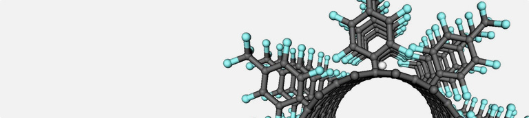
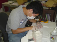
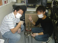
My project involved fabricating various nanostructures on the surface of a silicon substrate. Specifically, I was interested in growing a single-atom wide nanowire of silicon-29 on the surface of silicon-28. We did this by taking advantage of the 7x7 surface structure of silicon. By polishing the silicon wafer at a tilt and then annealing using DC current, we produced perfectly straight steps on the surface, which allowed us to deposit atoms in a controlled manner because of the large number of dangling bonds at the step edges. The results were then verified using scanning tunneling microscopy and spectroscopy.
I don’t think I will continue with this specific project in the future, but my experience in the lab helped me gain a better idea of the lifestyle of scientific research. The Itoh Lab is very international, so I also saw that as a scientist, there is plenty of opportunity to meet and work with people from all over the world. While before the summer I was not very sure of my future plans I think that this experience has made me more likely to pursue a research career in the future.
Lab Group Overview
The students of Itoh Lab are a very friendly and cohesive group, and we did many things together both in and out of the lab. Eating lunch and oftentimes dinner together was something that happened almost every day. English in the lab is generally very good, so language was never a problem.
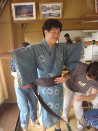
My mentor, Tomoya, and a number of other Itoh Lab group members (Shinchiang, Fumi, and Luis) were particularly helpful during my time in the lab. I had a great time working with them at school and also eating and travelling together outside of lab. Together, they taught me Japanese, showed me places to explore in Tokyo, and sampled a lot of the local food. I really felt like part of the group at Itoh lab and it really goes a long way if you spend some time getting to know each of the people in the lab, since they all have things to offer that will make your summer more interesting.
I did face some challenges in terms of my research project though. Part of this was due to equipment malfunction; the STM, which was the focus of my project, was broken the entire summer. Another reason was because there is not such an emphasis on independent research by undergraduates in the lab therefore my experience in the lab mostly consisted of being guided step-by-step by my mentor rather than being able to independently investigate a topic. The upside to this situation was that there was plenty of free time to pursue things that interested me. I spent a lot of time studying the theory of Silicon (111) 7x7 structures and spent some time dabbling in electron spin resonance (worked on by another group in the lab). There was also plenty of time to practice my Japanese with my labmates, to read about everything from science to politics and Japanese history, and of course to travel. As Itoh-sensei himself said, the experience at Keio is probably 20% nano research and 80% Japan.
Daily Life in Japan
Weekdays consisted of work at the lab. Hours were generally very flexible, with no two days being exactly the same, and most researchers (including undergraduate students) setting their own hours. Days generally start late, usually around noon, but also end late – anytime from 8:00 to 10:00 pm. Even though the hours were long, time at the lab consisted of a healthy mix of work, socializing and relaxing. My activities generally consisted of: polishing silicon wafers in the basement room, fiddling with the STM with my mentor, correcting English papers for my labmates, and interacting with the students in the student room upstairs. My labmates were a very friendly and cohesive group, and we often at lunch and dinner together.
Hiyoshi, where the Engineering campus of Keio University is located, is very close to Azabu-juban, the site of the NanoJapan orientation. So close that you probably don’t even need to ship your luggage; making 2 trips on the subway (25-minutes one way) is a lot cheaper than paying them to drive your bags. Since Hiyoshi is so close to Tokyo, I would strongly recommend getting a JR Rail Pass. It will be good because (1) the shinkansen network is so easily accessible and (2) it will let you see parts of Japan other than Tokyo. The AJALT language classes offered during the three-week orientaiton were REALLY useful; I was glad I paid attention, even though they were at 9:00 in the morning every day. It also helped me to try to speak Japanese as much as possible with my labmates and others in Japan. Keio University does not offer Japanese classes that you can take during the research internship period, but the Yokohama Kohoku International Lounge is just 10-minutes away at Kikuna station but you do need to be sure to sign up early if you want to study there as they go on summer break in mid-July. They also offer some Japanese culture classes such as a Tea Ceremony, Flower Arrangement, and Calligraphy.
Weekends were crazy. Crazy, but awesome. The four NanoJapan students in the Tokyo area (Georgia, Laura, Hsin-Zon, and me) travelled together every single weekend during the internship period and together we visited practically every place the shinkansen would take us - and some that it didn’t. Sleep didn’t always happen, and when it did it was short, but none of us regretted it. We often left Tokyo on Friday night, stayed overnight in youth hostels (cheap but good and clean), and returned to work at our labs Sunday evening or Monday morning.
My favorite experiences in Japan were...
Before I left for Japan I wish I had...
Taken a break after school to get into the Japan mindset, and taken some time to read more about Japan.
While I was in Japan I wish I had...
Spent less time relaxing during my first two weekends at the lab and more time going out and exploring and budgeted a little more carefully so I didn’t exceed my stipend by so much. But I don’t regret spending so much money because it really was a once-in-a-lifetime opportunity.
Tips for Future NanoJapan Participants